- English
- Español
- Português
- русский
- Français
- 日本語
- Deutsch
- tiếng Việt
- Italiano
- Nederlands
- ภาษาไทย
- Polski
- 한국어
- Svenska
- magyar
- Malay
- বাংলা ভাষার
- Dansk
- Suomi
- हिन्दी
- Pilipino
- Türkçe
- Gaeilge
- العربية
- Indonesia
- Norsk
- تمل
- český
- ελληνικά
- український
- Javanese
- فارسی
- தமிழ்
- తెలుగు
- नेपाली
- Burmese
- български
- ລາວ
- Latine
- Қазақша
- Euskal
- Azərbaycan
- Slovenský jazyk
- Македонски
- Lietuvos
- Eesti Keel
- Română
- Slovenski
- मराठी
- Srpski језик

China PCBA supplier, PCB assembly supplier, PCB assembly manufacturer China Manufacturers, Suppliers, Factory
We always follow the principle "Quality Very first, Prestige Supreme". We have been fully committed to delivering our customers with competitively priced high-quality products and solutions, prompt delivery and experienced services for PCBA supplier, PCB assembly supplier, PCB assembly manufacturer China, We guaranteed high-quality, if clients were not pleased together with the products' good quality, you can return inside of 7days with their original states.
PCBA supplier, PCB assembly supplier, PCB assembly manufacturer China, Our continual availability of high grade products in combination with our excellent pre-sale and after-sales service ensures strong competitiveness in an increasingly globalized market. welcome new and old customers from all walks of life to contact us for future business relationships and mutual success!
Related Products


Hot Products

PCBA Solder Paste Inspection
Hitech is a professional China PCBA Solder Paste Inspection manufacturer and supplier, Printed Circuit Board Assembly (PCBA) refers to the process of assembling electronic components onto a printed circuit board (PCB). A PCB is an electronic component that consists of conductive pathways, electronic components, and other elements assembled on a non-conductive substrate using printing techniques. PCBA involves soldering electronic components onto the PCB to complete the assembly and connection of circuits.
Multilayer PCB
Multilayer PCBs (Printed Circuit Boards) are a highly advanced and versatile type of PCB used in a wide range of industries, from consumer electronics to aerospace. They are designed with multiple layers of conductive copper traces and insulating material, providing a high level of complexity and functionality in a single PCB. Multilayer PCBs offer a wide range of benefits, making them an ideal choice for advanced electronic devices.
Plastic Injection Molding
Hitech is a professional Plastic Injection Molding suppliers in China. Plastic Injection Molding is a manufacturing process that has revolutionized the way we produce plastic products. It is a versatile and cost-effective method that allows for the creation of intricate and complex parts with high precision and accuracy.
Communication Device PCBA Board Assembly
Communication Device PCBA Board Assembly refers to the manufacturing process of printed circuit board assemblies (PCBAs) that are used in communication devices such as smartphones, tablets, routers, and other electronic devices that require wireless communication capabilities. The PCBA is a critical component of these devices as it houses the electronic components and circuitry that enable wireless communication.
Automotive PCBA Board Assembly
Automotive PCBA Board Assembly refers to the manufacturing process of printed circuit board assemblies (PCBAs) that are used in automotive applications. These PCBAs are critical components of modern automobiles, and are used in a variety of applications such as engine control units, infotainment systems, safety systems, and more.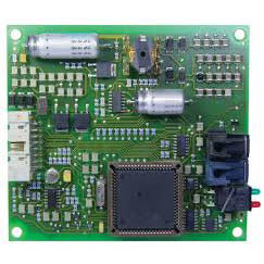
Custom Charging PCBA
In today's fast-paced world, the need for efficient and reliable power supply for electronic devices makes high-performance charging solutions essential. To meet the growing demand for customizable, high-performance charging, innovations in the HiTech field have led to the development of custom charging PCBA. These specialized printed circuit board assemblies are designed to deliver performance exceeding that of standard solutions.
- Related Blog
- Reviews