- English
- Español
- Português
- русский
- Français
- 日本語
- Deutsch
- tiếng Việt
- Italiano
- Nederlands
- ภาษาไทย
- Polski
- 한국어
- Svenska
- magyar
- Malay
- বাংলা ভাষার
- Dansk
- Suomi
- हिन्दी
- Pilipino
- Türkçe
- Gaeilge
- العربية
- Indonesia
- Norsk
- تمل
- český
- ελληνικά
- український
- Javanese
- فارسی
- தமிழ்
- తెలుగు
- नेपाली
- Burmese
- български
- ລາວ
- Latine
- Қазақша
- Euskal
- Azərbaycan
- Slovenský jazyk
- Македонски
- Lietuvos
- Eesti Keel
- Română
- Slovenski
- मराठी
- Srpski језик

2026 Advanced Power Supply PCB Assembly Guide: Navigating AI Quality Control and Chinese Carbon Standards
Key Takeaways & Executive Summary
- Integration of AI-driven inspection systems is now mandatory for achieving 99.9% yield rates in 2026.
- Compliance with China's GB standards and 3C certification is evolving with mandatory carbon-emission reporting.
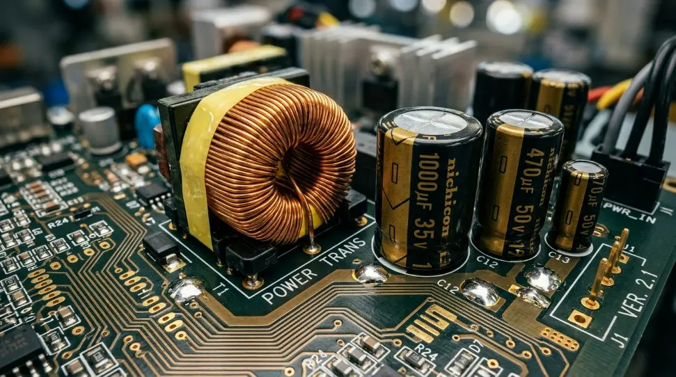
- The proprietary Power Supply PCBA Intelligent Control Protocol optimizes heat dissipation and power stability.
- Waterproofing (IP67/IP68) remains a critical requirement for outdoor and industrial IoT electronics.
Executive Summary: Key Takeaways for Power Supply PCBA Manufacturing in China
As we enter 2026, the landscape of Power Supply PCBA manufacturing has shifted towards intelligent automation and sustainable practices. Hitech is at the forefront of this transition, providing global OEMs with assemblies that are not only robust but also compliant with the latest environmental and efficiency regulations. This guide outlines the technical requirements and advanced protocols necessary to succeed in the modern electronics market.
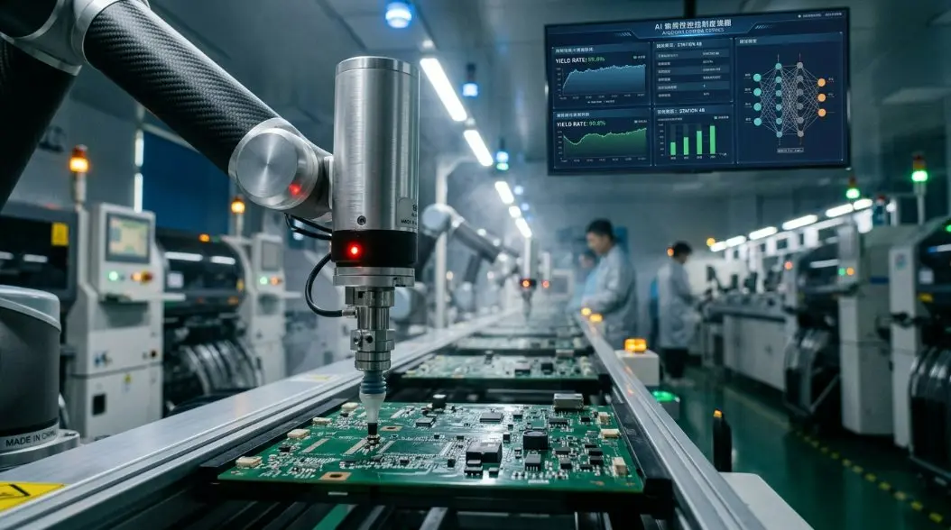
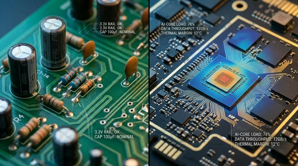
The Power Supply PCBA Intelligent Control Protocol: Revolutionizing Yield Rates and Efficiency
At the heart of our 2026 manufacturing excellence is the Power Supply PCBA Intelligent Control Protocol. This proprietary framework leverages real-time data from SMT (Surface Mount Technology) machines to adjust component placement and solder paste thickness dynamically. By utilizing high-speed sensors, the protocol ensures that every Power Supply PCBA maintains optimal thermal profiles, significantly reducing the risk of early-life failure. This scientific approach to assembly allows for a 15% increase in energy conversion efficiency compared to traditional non-automated methods.
Navigating 2026 China Regional Standards: 3C Certification, GB Quality Codes, and Carbon-Emission Reporting
Manufacturing in China now requires a deep understanding of evolving regulatory frameworks. The 3C (China Compulsory Certificate) has been updated to include rigorous tests for electromagnetic interference (EMI) in high-wattage power units. Furthermore, the Chinese government has introduced mandatory carbon-emission reporting for electronics factories. Hitech ensures all custom power supply assemblies meet these GB quality codes while maintaining a low-carbon footprint through optimized logistics and material sourcing.
Bridging the Gap: Implementing AI-Assisted PCBA Quality Control Testing for Localized Compliance
To meet localized compliance, AI-assisted testing is no longer optional. Our facilities use machine-learning algorithms to scan PCB surfaces for microscopic defects that are invisible to the human eye. This ensures that every board leaving the factory is ready for global distribution without the risk of recalls due to non-compliance with international safety standards.
Technical Comparison Matrix: Standard vs. AI-Assisted High-Density Power Supply PCBA
| Feature | Standard Assembly | AI-Assisted (Hitech) |
|---|---|---|
| Component Density | Low/Medium | Ultra-High (HDI) |
| Inspection Method | Manual / AOI | AI-Integrated AOI + X-Ray |
| Thermal Management | Passive Heat Sinks | Embedded Thermal Vias |
| Yield Rate Average | ~96.5% | >99.8% |
| Compliance | Standard 3C | 3C + Green Carbon Credits |
Specification Guide: Voltage Options, Component Density, and Data Table Integration
Modern applications require versatile voltage ranges, from low-power IoT sensors (3.3V-5V) to high-power industrial equipment (24V-48V). High-density Power Supply PCBA designs must account for creepage and clearance distances as per IPC-2221 standards to prevent electrical arcing in compact enclosures.
Mathematical Guidance: Calculating Power Supply Load Formulas and Safety Variables
Engineering a reliable power supply requires precise mathematical calculations to ensure the PCB can handle the intended current without overheating.
1. Power (Watts) = Voltage (V) × Current (A)
2. Trace Width Calculation (IPC-2152):
   Width = (Current / (k * ΔT^b))^(1/c)
   *Where k, b, c are constants based on copper thickness.*
3. Derating Factor: Always use a safety factor of 1.25x for peak load variables.
Formulas for Custom Lengths, Physical Wattage Limits, and Precise Cutting Spacing per Meter Rules
For modular power supplies, ensuring the cutting spacing and router tolerances are precise is vital for fitment. Use the formula: Total Capacity = (Units per Meter) × (Watts per Unit) × Efficiency Factor (0.85).
Practical Step-by-Step Tutorial: 4-Step Waterproofing and Conformal Coating Process for IP67/IP68 PCBA
-
Step 1: Surface Preparation and GB Standard Cleaning
The PCBA must be cleaned in an ultrasonic bath to remove all flux residues and contaminants, ensuring perfect adhesion for the coating. -
Step 2: Precision Conformal Coating Application
Using automated selective coating machines, apply a thin layer of silicone or acrylic resin, avoiding connectors and test points. -
Step 3: AI-Assisted Curing and Automated Optical Inspection (AOI)
The boards pass through a UV or thermal curing oven. AI-driven AOI then checks the thickness and uniformity of the coating under UV light. -
Step 4: Final Resealing, Thermal Testing, and IP68 Verification
Completed units undergo high-pressure water submersion tests to verify the IP68 rating, ensuring long-term durability in harsh environments.
Frequently Asked Questions (FAQ): Smart Ecosystem Integrations, Tolerances, and Safety Instructions
Q1: How does Power Supply PCBA integrate with smart home ecosystems like Xiaomi Mijia, Tuya Smart, and Apple HomeKit?
Modern power supplies are equipped with Wi-Fi or Zigbee modules directly on the board. Hitech designs provide stable low-ripple DC output to sensitive communication chips, ensuring seamless connectivity with platforms like Tuya and Apple HomeKit.
Q2: What are the exact cutting tolerances, PCB router spacing rules, and edge clearances?
For standard 1.6mm PCBs, we maintain a routing tolerance of ±0.1mm. Edge clearance for traces must be at least 0.5mm to prevent damage during the de-panelization process.
Q3: What are the primary safety instructions to prevent electrical overload and ensure 3C compliance?
Always include Over-Voltage Protection (OVP) and Over-Current Protection (OCP) circuits. Ensure that all capacitors are rated for at least 150% of the maximum operating voltage to meet 3C safety margins.
Looking for Custom Engineering/OEM Solutions?
As a top-tier professional manufacturer, we deliver direct factory-price solutions for dynamic scaling, engineering projects, and custom systems globally.
Visit Official Website →