- English
- Español
- Português
- русский
- Français
- 日本語
- Deutsch
- tiếng Việt
- Italiano
- Nederlands
- ภาษาไทย
- Polski
- 한국어
- Svenska
- magyar
- Malay
- বাংলা ভাষার
- Dansk
- Suomi
- हिन्दी
- Pilipino
- Türkçe
- Gaeilge
- العربية
- Indonesia
- Norsk
- تمل
- český
- ελληνικά
- український
- Javanese
- فارسی
- தமிழ்
- తెలుగు
- नेपाली
- Burmese
- български
- ລາວ
- Latine
- Қазақша
- Euskal
- Azərbaycan
- Slovenský jazyk
- Македонски
- Lietuvos
- Eesti Keel
- Română
- Slovenski
- मराठी
- Srpski језик

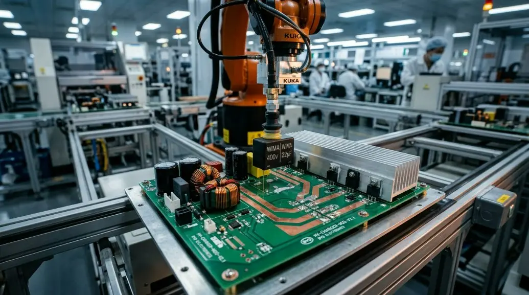
PCB Assembly in China factory: 2026 EV Infrastructure & GaN Fast-Charging PCBA for Southeast Asia
As the Southeast Asian (ASEAN) market pivots toward a greener future, the demand for high-performance electronic components has reached an all-time high. By 2026, the regional EV infrastructure is expected to undergo a massive transformation, requiring robust and efficient Custom Charging PCBA solutions. For businesses in Malaysia, Thailand, and Indonesia, partnering with a high-tech China factory for PCB assembly ensures access to cutting-edge technology and cost-effective manufacturing.
Why Choose Southeast Asia for Next-Gen EV and GaN PCB Assembly?
Southeast Asia is uniquely positioned as a global hub for EV adoption due to favorable government incentives and a rapidly growing middle class. Leveraging China-based PCB Assembly expertise allows regional companies to integrate advanced Gallium Nitride (GaN) technology into their local supply chains, significantly reducing charging times and increasing power density for consumer and industrial applications.
Capitalizing on ASEAN Localized Supply Chain Resilience
Post-pandemic shifts have emphasized the need for resilient supply chains. By sourcing PCBA from specialized factories in China that understand the ASEAN logistics corridor, brands can maintain steady production schedules despite global volatility. This synergy facilitates a faster time-to-market for innovative power electronics across Vietnam, Singapore, and beyond.
Addressing the 2026 EV Charging Infrastructure Boom
The year 2026 marks a critical milestone for EV infrastructure projects in the Philippines and Thailand. High-voltage PCBAs designed for DC fast chargers and Level 2 AC stations are essential. Our factory focuses on high-reliability designs that withstand the tropical humidity and thermal stress common in Southeast Asian climates.
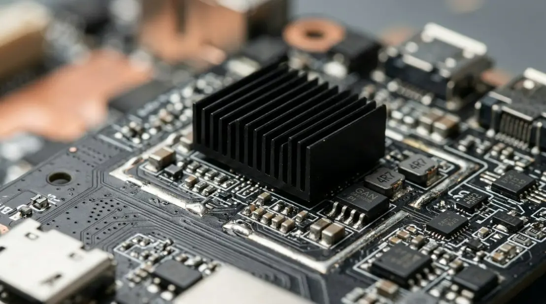
Next-Gen GaN Fast-Charging PCB Assembly Solutions
GaN technology is revolutionizing the power adapter market. By replacing traditional silicon with Gallium Nitride, chargers become smaller, cooler, and more efficient. Our facility specializes in the precision assembly required for GaN components, ensuring that your custom charging projects meet the high-frequency demands of modern fast-charging protocols.
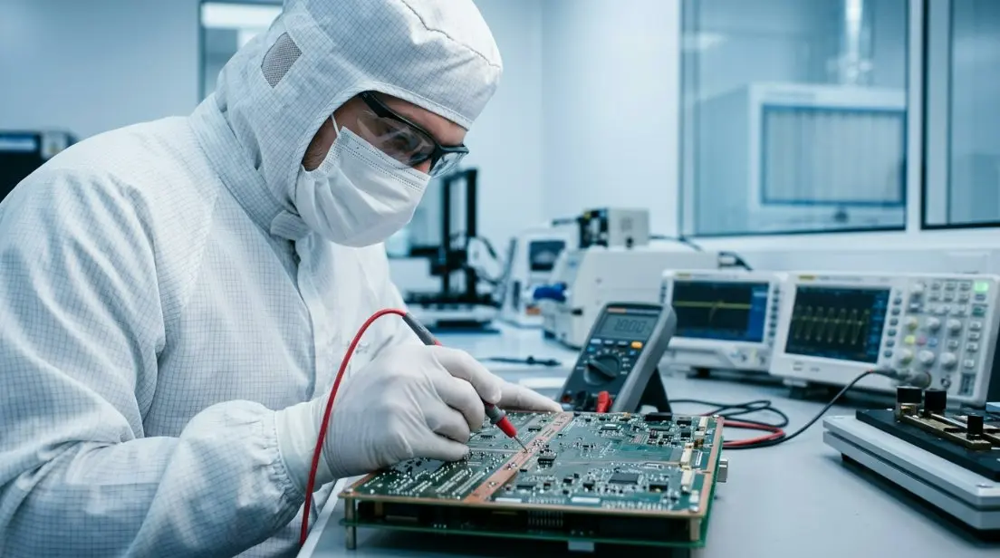
Local ASEAN Electrical Compliance and Certifications
Entering the ASEAN market requires more than just high-quality hardware; it requires strict adherence to local safety standards. Our manufacturing process incorporates comprehensive testing phases to ensure every board is ready for regional certification.
Navigating SIRIM (Malaysia), TISI (Thailand), and SNI (Indonesia) Standards
Each country in Southeast Asia has its own regulatory body. Whether it is SIRIM in Malaysia, TISI in Thailand, or SNI in Indonesia, our PCBA services include rigorous quality control checks that align with these specific electrical safety and performance requirements, easing the path to market entry.
IATF 16949 Automotive Compliance for EV PCBA Manufacturing
For the automotive sector, IATF 16949 certification is non-negotiable. Our China factory maintains these standards to ensure that every Custom Charging PCBA intended for EV use meets the zero-defect quality management principles necessary for passenger safety.
Data Specs Table: EV and GaN PCBA Capabilities in Southeast Asia
To help you understand the technical scope of our services, the following table outlines our core capabilities for high-power electronics projects.
| Parameter | Specification Details |
|---|---|
| PCB Material | FR-4 High TG, Rogers, Ceramic, Aluminum Base |
| Copper Weight | 2oz - 10oz (Heavy Copper for EV Charging) |
| Layer Count | 1 to 32 Layers |
| GaN Support | Optimized for Navitas, GaN Systems, Power Integrations |
| Thermal Management | Thermal vias, metal cores, and specialized TIM application |
High-Voltage PCB Material and Heavy Copper Specifications
EV charging requires boards that can handle significant current without excessive heat buildup. We utilize heavy copper traces and specialized substrates to ensure long-term durability and safety in high-voltage environments.
Thermal Management Metrics for GaN Power Adapters
Efficient heat dissipation is the biggest challenge in GaN design. Our assembly process focuses on optimized component placement and thermal interface material (TIM) application to keep temperatures within safe operating limits, even in 100W+ fast chargers.
Cost-Efficiency and Geographic Arbitrage in ASEAN Electronics Manufacturing
By manufacturing in China and distributing across ASEAN, companies can take advantage of geographic arbitrage—benefiting from China's mature component ecosystem while serving the high-growth markets of Southeast Asia.
Overcoming Global Component Supply Constraints with Localized Sourcing
Our deep relationships with Tier-1 component distributors in Asia allow us to bypass many of the supply chain bottlenecks that affect Western manufacturers. This ensures that your EV and GaN projects stay on track for the 2026 infrastructure wave.
How to Start Your Specialized PCBA Project in Southeast Asia
Ready to bring your power electronics to the ASEAN market? The process is simple: provide your Gerber files and BOM list, and our engineering team will perform a DFM (Design for Manufacturing) review. We specialize in prototyping and mass production, ensuring your custom charging solutions are ready for the competitive 2026 landscape.