- English
- Español
- Português
- русский
- Français
- 日本語
- Deutsch
- tiếng Việt
- Italiano
- Nederlands
- ภาษาไทย
- Polski
- 한국어
- Svenska
- magyar
- Malay
- বাংলা ভাষার
- Dansk
- Suomi
- हिन्दी
- Pilipino
- Türkçe
- Gaeilge
- العربية
- Indonesia
- Norsk
- تمل
- český
- ελληνικά
- український
- Javanese
- فارسی
- தமிழ்
- తెలుగు
- नेपाली
- Burmese
- български
- ລາວ
- Latine
- Қазақша
- Euskal
- Azərbaycan
- Slovenský jazyk
- Македонски
- Lietuvos
- Eesti Keel
- Română
- Slovenski
- मराठी
- Srpski језик

China IOT PCBA Manufacturers, Suppliers, Factory
Getting buyer gratification is our company's purpose endlessly. We will make good attempts to produce new and top-quality products, meet up with your specific requirements and provide you with pre-sale, on-sale and after-sale expert services for IOT PCBA,IOT pcb design, In case you have any comments about our corporation or products, you should experience no cost to call us, your coming mail will be remarkably appreciated.
IOT PCBA, We will continue to devote ourselves to market & product development and build a well-knit service to our customer to create a more prosperous future. Make sure you contact us today to find out how we can work together.
Related Products


Hot Products

BGA PCB Assembly
When it comes to designing and manufacturing electronic devices, the printed circuit board (PCB) is an essential component. It connects all the electronic components and serves as the backbone of the device. However, the performance of the device largely depends on the quality of the PCB assembly. That's where BGA PCB assembly comes in.
Controller PCBA Board Assembly
Controller PCBA Board Assembly: Streamline Your Electronic Device Production Electronic devices that require controllers are ubiquitous and are used in a wide range of applications, including industrial automation, robotics, and consumer electronics. In order to ensure that these devices function smoothly and efficiently, it's important to have a high-quality controller PCB assembly (PCBA) in place. This is where our controller PCBA board assembly service comes in.
PCBA X-RAY Testing
Hitech as a professional high quality PCBA X-RAY Testing manufacturer, Printed Circuit Board Assembly (PCBA) X-ray testing is a non-destructive testing method used to inspect the internal structure of a PCB. It is a crucial process in the manufacturing of electronic devices, ensuring that the final product is of high quality, free from defects, and functions as intended. X-ray testing uses specialized equipment to generate images of the internal structure of the PCB, allowing manufacturers to identify defects such as voids in solder joints, short circuits, and open connections.
Automated Equipment PCBA Board Assembly
Our products are have in stock of factory, welcome to wholesale Automated Equipment PCBA Board Assembly from Hitech. Automated equipment PCBA board assembly refers to the use of automated machines in the manufacturing process of printed circuit board assemblies (PCBAs). Automated equipment is used to place components onto the PCB, solder them in place, and perform other manufacturing tasks, such as testing and quality control.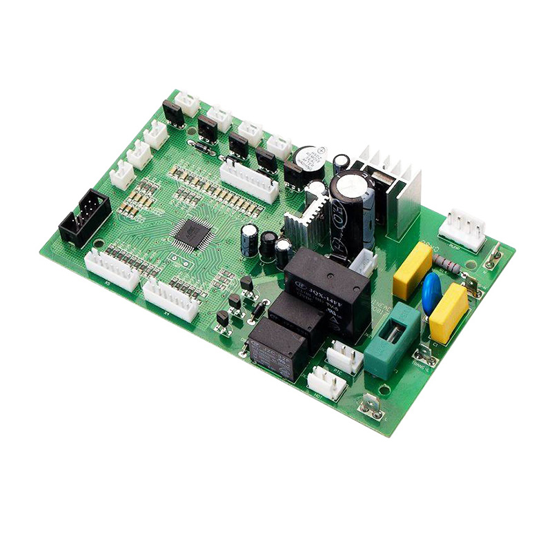
IOT PCB Design And Layout
You are welcomed to come to our factory to buy the latest selling, low price, and high-quality IOT PCB design and layout, Hitech looks forward to cooperating with you.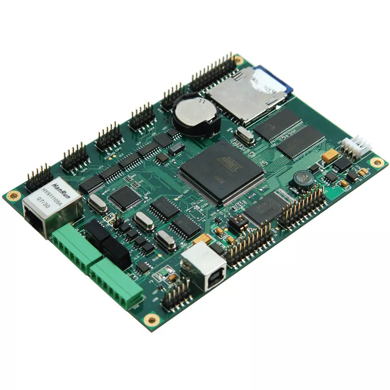
Custom PCB Assembly and Prototype PCBA
As a professional PCB manufacturer and supplier in China, Hitech focuses on high-quality Custom PCB Assembly and Prototype PCBA, strictly adhering to IPC standards. Our own factory is equipped with advanced equipment, specializing in SMT, DIP, and BGA processes, enabling rapid delivery of R&D and small-batch orders within 24-72 hours. High cost-effectiveness and flexibility, covering the entire process, have earned the trust of customers worldwide.
- Related Blog
- Reviews