- English
- Español
- Português
- русский
- Français
- 日本語
- Deutsch
- tiếng Việt
- Italiano
- Nederlands
- ภาษาไทย
- Polski
- 한국어
- Svenska
- magyar
- Malay
- বাংলা ভাষার
- Dansk
- Suomi
- हिन्दी
- Pilipino
- Türkçe
- Gaeilge
- العربية
- Indonesia
- Norsk
- تمل
- český
- ελληνικά
- український
- Javanese
- فارسی
- தமிழ்
- తెలుగు
- नेपाली
- Burmese
- български
- ລາວ
- Latine
- Қазақша
- Euskal
- Azərbaycan
- Slovenský jazyk
- Македонски
- Lietuvos
- Eesti Keel
- Română
- Slovenski
- मराठी
- Srpski језик

Products


IOT PCB Design And Layout
You are welcomed to come to our factory to buy the latest selling, low price, and high-quality IOT PCB design and layout, Hitech looks forward to cooperating with you.
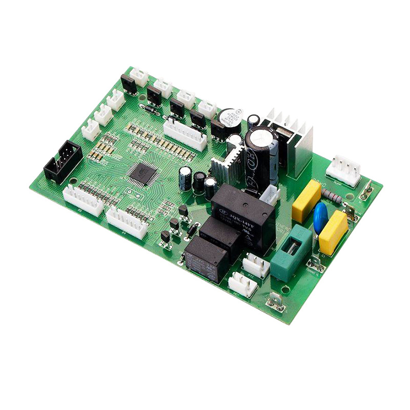
Model:Hitech-PCB design 1
Send Inquiry
Product Description
IoT PCB Design and Layout are essential elements in the development of IoT devices. These boards are specifically designed to facilitate the integration of electronics and wireless communication, making it possible to create a wide range of IoT devices.
IoT PCB Layout involves the creation of a highly optimized circuit board for IoT applications. This process includes designing a compact and energy-efficient board that can accommodate multiple sensors, microcontrollers, antennas, and other electronic components in a small form-factor.
To create an optimal IoT PCB Layout, designers must consider the following:Power consumption: IoT devices are often battery-powered, and therefore, must be designed to minimize power usage. Low-power components, efficient power management techniques and battery-saving features must be incorporated into the PCB design.RF Design: PCB layout and antenna placement play a significant role in a device’s wireless performance. The proper design of trace lengths, spacing between traces, and antenna placement must be taken into account.Standard Interface Support: Incorporating standard interfaces like USB, Ethernet, and Wi-Fi in the IoT PCB design makes it easier for users to access and communicate with the device.Security: IoT devices are vulnerable to security threats and are at risk of being hacked. Designers must build security features like encryption, authentication, and authorization into the PCB design.Durability: The PCB layout must be designed for long-term reliability in harsh environments. This means using high-quality materials, mounting styles, and coatings that provide durability against moisture, dust, and temperature extremes.At our company, we are dedicated to providing exceptional IoT PCB design and layout services. Our team of experienced designers possesses the skills and expertise to design PCBs for IoT devices that meet or exceed industry standards. We optimize designs for power efficiency, wireless connectivity, and security, resulting in high-quality IoT products that meet our clients' unique requirements.
In summary, IoT PCB design and layout is a complex process that requires careful consideration of power consumption, RF design, standard interface support, security, and durability. Partnering with an experienced IoT PCB design and layout service provider is essential to ensure the creation of safe, reliable, and optimized IoT devices.
Hot Tags: IOT PCB design and layout, China, Suppliers, Factory, Manufacturers, Customized
Product Tag
Related Category
Send Inquiry
Please feel free to give your inquiry in the form below. We will reply you in 24 hours.