- English
- Español
- Português
- русский
- Français
- 日本語
- Deutsch
- tiếng Việt
- Italiano
- Nederlands
- ภาษาไทย
- Polski
- 한국어
- Svenska
- magyar
- Malay
- বাংলা ভাষার
- Dansk
- Suomi
- हिन्दी
- Pilipino
- Türkçe
- Gaeilge
- العربية
- Indonesia
- Norsk
- تمل
- český
- ελληνικά
- український
- Javanese
- فارسی
- தமிழ்
- తెలుగు
- नेपाली
- Burmese
- български
- ລາວ
- Latine
- Қазақша
- Euskal
- Azərbaycan
- Slovenský jazyk
- Македонски
- Lietuvos
- Eesti Keel
- Română
- Slovenski
- मराठी
- Srpski језик

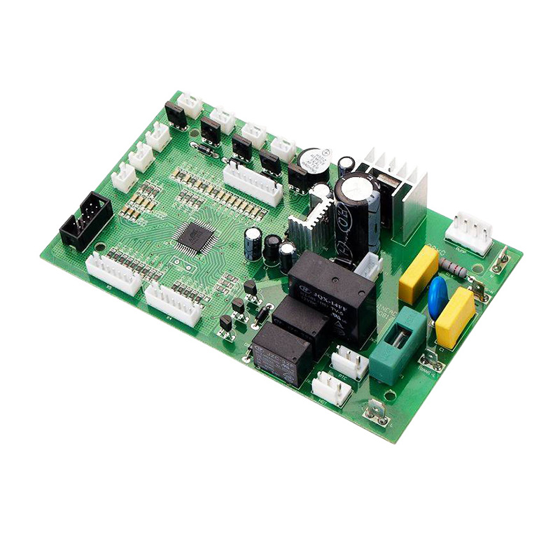
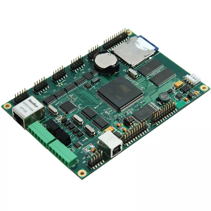
China EMS Supplier Box Build Assembly Manufacturers, Suppliers, Factory
Together with the "Client-Oriented" enterprise philosophy, a arduous good quality control technique, sophisticated producing equipment and a sturdy R&D staff, we generally offer superior quality merchandise, superb solutions and aggressive rates for EMS Supplier Box Build Assembly,Magnetic Shuttering Formwork Concrete Magnet Box,Electronics Assembly and Shenzhen Box Build,Shenzhen Electronic Box Build Assembly,Assembly Box Build Contract Manufacturing, For anyone who is fascinated in any items, be sure to truly feel totally free to speak to us for further more details or be sure to deliver us email immediately, we will reply you in 24 hrs as well as the most effective quotation will probably be provided.
EMS Supplier Box Build Assembly, We honor ourselves as a company that comprises of a strong team of professionals who are innovative and well experienced in the international trading, business development and product advancement. Moreover, the company stays unique among its competitors due to its superior standard of quality in production, and its efficiency and flexibility in business support.
Related Products


Hot Products

PCB Layout
Printed Circuit Board (PCB) layout is an integral part of the electronic design process. It involves placing components and routing traces on a PCB to ensure that the final product meets the desired specifications. PCB layout is a critical step in the electronic design process, which can impact the performance, manufacturability, and reliability of the final product. In this article, we will explore the importance of PCB layout and how it can impact the overall success of your project
Silicone Injection Molding
Silicone Injection Molding is a manufacturing process that involves injecting liquid silicone into a mold under high pressure and temperature to produce silicone rubber parts. This process is used to produce a wide range of silicone products such as seals, gaskets, keypads, and other rubber components.
Communication Device PCBA Board Assembly
Communication Device PCBA Board Assembly refers to the manufacturing process of printed circuit board assemblies (PCBAs) that are used in communication devices such as smartphones, tablets, routers, and other electronic devices that require wireless communication capabilities. The PCBA is a critical component of these devices as it houses the electronic components and circuitry that enable wireless communication.
Rigid-Flexible PCB
As the professional manufacture, Hitech would like to provide you Rigid-Flexible PCB. A rigid-flexible PCB is a printed circuit board that combines both rigid and flexible materials in a single board. Rigid-flex PCBs are designed to provide the benefits of both rigid and flexible PCBs, allowing for greater design flexibility and functionality.
Bluetooth Tracker PCBA Design
One of Chinese manufacturer of Bluetooth Tracker PCBA Design, offering excellent quality at a competitive price, is Hitech. Feel free to get in touch.
Introduction to Our Expertise in PCB Design
In today's rapidly advancing technological landscape, Printed Circuit Board (PCB) design plays a pivotal role in the development of modern electronics and systems. At our company, we pride ourselves as leaders in introduction to Our Expertise in PCB Design, a field that involves the strategic layout and assembly of electronic components on a flat surface to ensure optimal performance and functionality.
- Related Blog
- Reviews