- English
- Español
- Português
- русский
- Français
- 日本語
- Deutsch
- tiếng Việt
- Italiano
- Nederlands
- ภาษาไทย
- Polski
- 한국어
- Svenska
- magyar
- Malay
- বাংলা ভাষার
- Dansk
- Suomi
- हिन्दी
- Pilipino
- Türkçe
- Gaeilge
- العربية
- Indonesia
- Norsk
- تمل
- český
- ελληνικά
- український
- Javanese
- فارسی
- தமிழ்
- తెలుగు
- नेपाली
- Burmese
- български
- ລາວ
- Latine
- Қазақша
- Euskal
- Azərbaycan
- Slovenský jazyk
- Македонски
- Lietuvos
- Eesti Keel
- Română
- Slovenski
- मराठी
- Srpski језик

China PCB assembly Manufacturers, Suppliers, Factory
We'll dedicate ourselves to offering our esteemed customers together with the most enthusiastically thoughtful solutions for PCB assembly,remote controller PCBA,pcba, "Passion, Honesty, Sound service, Keen cooperation and Development" are our objectives. We have been here anticipating good friends all over the environment!
PCB assembly, Our goods have been obtained more and more recognition from foreign clients, and established long term and cooperative relationship with them. We`ll offer the best service for every customer and sincerely welcome friends to work with us and establish the mutual benefit together.
Related Products


Hot Products
FR4 PCB
FR4 PCBs (Printed Circuit Boards) are one of the most widely used types of PCBs in the electronics industry. They are made from a material called FR4, which is a type of glass-reinforced epoxy laminate. FR4 is known for its excellent electrical insulation properties, high strength, and resistance to heat and moisture. These properties make FR4 PCBs an ideal choice for a wide range of applications, including consumer electronics, medical devices, industrial equipment, and more.
Multilayer PCB
Multilayer PCBs (Printed Circuit Boards) are a highly advanced and versatile type of PCB used in a wide range of industries, from consumer electronics to aerospace. They are designed with multiple layers of conductive copper traces and insulating material, providing a high level of complexity and functionality in a single PCB. Multilayer PCBs offer a wide range of benefits, making them an ideal choice for advanced electronic devices.
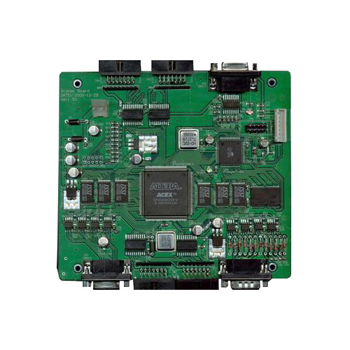
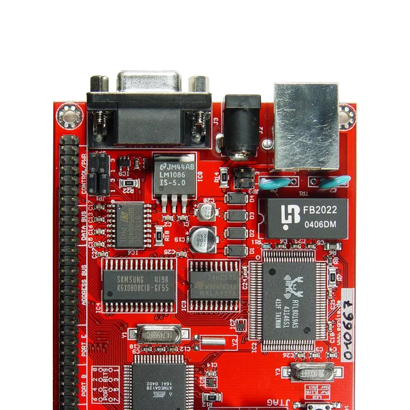
Communication Device PCBA Board Assembly
Communication Device PCBA Board Assembly refers to the manufacturing process of printed circuit board assemblies (PCBAs) that are used in communication devices such as smartphones, tablets, routers, and other electronic devices that require wireless communication capabilities. The PCBA is a critical component of these devices as it houses the electronic components and circuitry that enable wireless communication.
Rigid-Flexible PCB
As the professional manufacture, Hitech would like to provide you Rigid-Flexible PCB. A rigid-flexible PCB is a printed circuit board that combines both rigid and flexible materials in a single board. Rigid-flex PCBs are designed to provide the benefits of both rigid and flexible PCBs, allowing for greater design flexibility and functionality.
Box Build
Hitech is China manufacturer & supplier who mainly produces Box Build with many years of experience. Hope to build business relationship with you.
Bluetooth Speaker PCB Assembly
In today's digital age, the demand for portable and high-quality audio devices is ever-increasing. Behind the sleek exterior of these devices lies a complex system of components, with the PCB (Printed Circuit Board) assembly playing a important role in the functionality of the Bluetooth Speaker PCB Assembly.
- Related Blog
- Reviews