- English
- Español
- Português
- русский
- Français
- 日本語
- Deutsch
- tiếng Việt
- Italiano
- Nederlands
- ภาษาไทย
- Polski
- 한국어
- Svenska
- magyar
- Malay
- বাংলা ভাষার
- Dansk
- Suomi
- हिन्दी
- Pilipino
- Türkçe
- Gaeilge
- العربية
- Indonesia
- Norsk
- تمل
- český
- ελληνικά
- український
- Javanese
- فارسی
- தமிழ்
- తెలుగు
- नेपाली
- Burmese
- български
- ລາວ
- Latine
- Қазақша
- Euskal
- Azərbaycan
- Slovenský jazyk
- Македонски
- Lietuvos
- Eesti Keel
- Română
- Slovenski
- मराठी
- Srpski језик

China bluetooth PCBA Manufacturers, Suppliers, Factory
Often customer-oriented, and it's our ultimate target to become not only probably the most reputable, trustable and honest provider, but also the partner for our customers for bluetooth PCBA,bluetooth tracker PCBA,PCBA design, Seeing believes! We sincerely welcome the new prospects abroad to set up company interactions and also expect to consolidate the interactions with all the long-established clients.
bluetooth PCBA, During the short years, we serve our clients honestly as Quality First, Integrity Prime, Delivery Timely, which has earned us an outstanding reputation and an impressive client care portfolio. Looking forward to working with you Now!
Related Products


Hot Products

PCBA Automated Optical Inspection
Hitech as the professional manufacturer, we would like to provide you high quality PCBA Automated Optical Inspection. PCBA Automated Optical Inspection (AOI) is a technology used in the manufacturing process of Printed Circuit Board Assemblies to automatically inspect and identify defects or anomalies in the soldering and component placement.
Reflow Soldering PCB Assembly
Hitech is a professional leader China Reflow Soldering PCB Assembly manufacturer with high quality and reasonable price. It is a method used to join the surface mount components to the PCB using solder paste. Reflow soldering involves heating the PCB assembly to a specific temperature, melting the solder paste and creating a permanent joint between the component and the PCB. The process is highly precise, allowing for the creation of high-quality and reliable PCBAs that are used in a wide range of electronic devices. Reflow soldering is a key element in the manufacturing process of PCBAs, ensuring that the final product is of high quality, free from defects, and functions as intended.
Multilayer PCB
Multilayer PCBs (Printed Circuit Boards) are a highly advanced and versatile type of PCB used in a wide range of industries, from consumer electronics to aerospace. They are designed with multiple layers of conductive copper traces and insulating material, providing a high level of complexity and functionality in a single PCB. Multilayer PCBs offer a wide range of benefits, making them an ideal choice for advanced electronic devices.
Silicone Injection Molding
Silicone Injection Molding is a manufacturing process that involves injecting liquid silicone into a mold under high pressure and temperature to produce silicone rubber parts. This process is used to produce a wide range of silicone products such as seals, gaskets, keypads, and other rubber components.
Electronic Manufacturing Service
Electronic Manufacturing Service (EMS) is a complete solution for outsourcing the manufacturing of electronic products. This service includes a range of activities, from design and prototyping to final assembly, testing, and shipping. EMS providers work with original equipment manufacturers (OEMs) and other companies to provide a one-stop-shop for the entire electronics manufacturing process.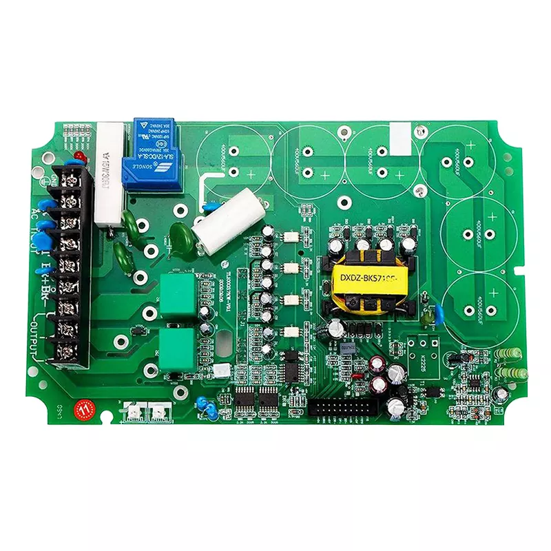
Turnkey PCBA Manufacturing Service
Hitech, a professional manufacturer deeply rooted in the Turnkey PCBA Manufacturing Service field, leverages China's complete electronics manufacturing industry chain to provide a one-stop Turnkey PCBA service covering PCB manufacturing, component procurement, SMT/DIP assembly, full-process testing, and global delivery. We strictly adhere to international standards such as ISO 9001, IPC, and RoHS. With a stable supply chain and automated production capabilities, we provide highly reliable and cost-effective customized solutions for customers in the industrial, medical, and consumer electronics sectors, becoming a trusted PCBA supplier globally.
- Related Blog
- Reviews