- English
- Español
- Português
- русский
- Français
- 日本語
- Deutsch
- tiếng Việt
- Italiano
- Nederlands
- ภาษาไทย
- Polski
- 한국어
- Svenska
- magyar
- Malay
- বাংলা ভাষার
- Dansk
- Suomi
- हिन्दी
- Pilipino
- Türkçe
- Gaeilge
- العربية
- Indonesia
- Norsk
- تمل
- český
- ελληνικά
- український
- Javanese
- فارسی
- தமிழ்
- తెలుగు
- नेपाली
- Burmese
- български
- ລາວ
- Latine
- Қазақша
- Euskal
- Azərbaycan
- Slovenský jazyk
- Македонски
- Lietuvos
- Eesti Keel
- Română
- Slovenski
- मराठी
- Srpski језик

2026 Blueprint: Advanced Quick Turn PCB Assembly & AI-Monitored SMT Production in China

Key Takeaways & Executive Summary
- Shift toward 100% transparent supply chain tracking for B2B stakeholders by mid-2026.
- Integration of the QuickTurn-Sync AI Precision Protocol for zero-defect SMT placement.
- Mandatory compliance with updated GB quality codes and 3C certification for high-voltage IoT boards.
- Acceleration of rapid prototyping cycles from 5 days down to 24-48 hours for complex multi-layer designs.
In the rapidly evolving landscape of 2026, the demand for precision and speed in electronics manufacturing has reached an all-time high. Our approach to quick turn pcb assembly integrates cutting-edge automation with deep technical expertise to ensure your designs transition from Gerber files to functional hardware with unprecedented efficiency. By leveraging the latest Introduction to Our Expertise in PCB Design, we provide a robust foundation for global tech innovators.
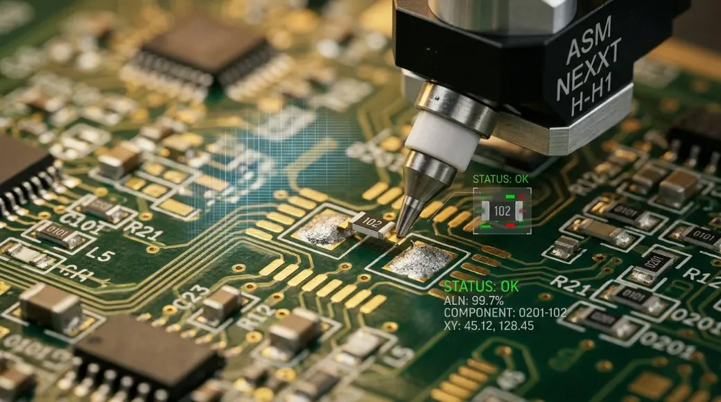
Introducing the QuickTurn-Sync AI Precision Protocol: Proprietary Real-Time SMT Monitoring
To meet the rigorous demands of next-generation hardware, we have pioneered the QuickTurn-Sync AI Precision Protocol. This proprietary system utilizes high-speed optical sensors and machine learning algorithms to monitor the Surface Mount Technology (SMT) process in real-time. Unlike traditional inspection, QuickTurn-Sync predicts potential solder bridge errors before they occur, adjusting nozzle pressure and placement coordinates in milliseconds. This level of quick turn pcb assembly ensures that even the most densely packed IoT boards maintain 99.99% yield rates during high-velocity production runs.
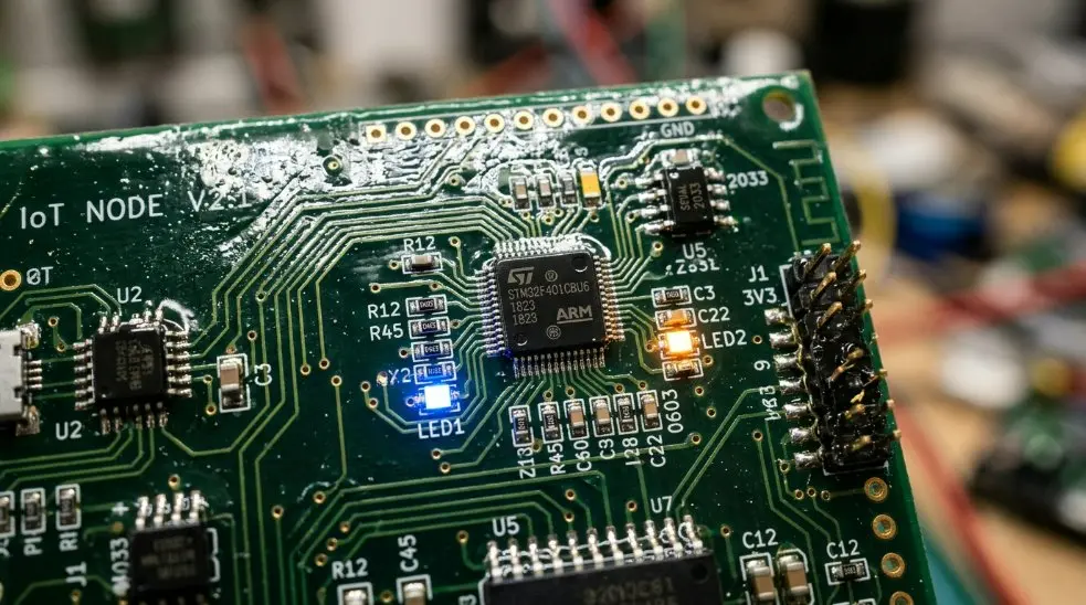
Practical Step-by-Step Tutorial: From Instant DFM Quotes to Final IoT Board Assembly
Navigating the path from concept to completion requires a structured methodology. Here is our 2026-optimized workflow for professional engineering teams:
Step 1: Uploading Gerber & BOM for AI-Powered Instant DFM Analysis
The journey begins with our digital interface. Once you upload your Gerber X3 files and Bill of Materials (BOM), our AI engine performs an instant Design for Manufacturing (DFM) analysis. It identifies clearance issues, annular ring violations, and thermal relief bottlenecks, providing a red-flag report in minutes.
Step 2: Component Sourcing Automation & Traceability Verification
Leveraging our quick turn pcb assembly supply chain network, we automate component procurement. Each part is verified for authenticity using blockchain-backed traceability, ensuring that no counterfeit silicon enters the production stream.
Step 3: Rapid SMT Pick-and-Place Setup for Smart Lighting Integrations
For smart lighting projects, we utilize specialized feeders for RGBIC LEDs. Our machines are calibrated for high-speed placement, ensuring that timing controllers and driver ICs are mounted with micron-level accuracy.
Step 4: IP67/IP68 Waterproof Conformal Coating and Resealing Process
Post-assembly, boards destined for outdoor or industrial use undergo an automated conformal coating process. Using specialized resins, we ensure your quick turn pcb assembly meets IP67 or IP68 standards for environmental resilience.
Technical Comparison Matrix: Standard Manufacturing vs. Quick Turn PCB Assembly for IoT
| Feature | Standard Manufacturing | Quick Turn (AI-Monitored) |
|---|---|---|
| Turnaround Time | 15-25 Business Days | 24-72 Hours |
| DFM Feedback | Manual (24h Delay) | Instant AI-Generated |
| Monitoring | Post-Production AOI | Real-Time QuickTurn-Sync |
| IoT Optimization | General Purpose | Specialized RGBIC & RF Tuning |
Specification Guide: Standard vs. RGBIC Capabilities and Voltage Options
When designing for advanced lighting, it is crucial to distinguish between standard LED strips and RGBIC (Individually Addressable) systems. Our 2026 lines support multi-voltage inputs (5V, 12V, 24V) with integrated level shifters to maintain signal integrity over long trace lengths.
Mathematical & Electrical Calculation Guidance: Safety Variables for PCB Engineering
Engineering precision is the hallmark of a successful quick turn pcb assembly. Use the following formulas to validate your trace widths and power requirements:
// Formula 1: Maximum Trace Current (IPC-2111 Standard)
I = k * dT^0.44 * A^0.725
// Where k is a constant, dT is temp rise, and A is cross-sectional area.

// Formula 2: Trace Impedance for High-Speed IoT Signals
Z0 = (87 / sqrt(Er + 1.41)) * ln(5.98h / (0.8w + t))
// h = dielectric thickness, w = trace width, t = trace thickness.
Navigating China Regional Standards: 3C Certification, GB Quality Codes, and OEM Technical Specs
For products entering the Chinese market or being manufactured within the region, compliance with the GB (Guobiao) standards is non-negotiable. Our quick turn pcb assembly processes align with GB/T 4588.3 for design requirements and GB 4943.1 for IT equipment safety.
Compliance Checks: Precise Cutting Spacing Per Meter Rules and Physical Wattage Limits
We strictly adhere to precise cutting spacing rules to ensure that modular boards can be separated without damaging internal copper planes. Furthermore, wattage limits are calculated to prevent thermal runaway in high-density enclosures, a critical factor for professional PCB assembly in the industrial sector.
Frequently Asked Questions (FAQ) on Quick Turn PCB Assembly
How does quick turn PCB assembly ensure compatibility with smart home ecosystems like Xiaomi Mijia, Tuya Smart, and Apple HomeKit?
Compatibility is achieved through specialized RF testing and the integration of certified wireless modules (Zigbee, Matter, or Wi-Fi). Our AI-monitored process ensures that the antenna impedance is matched perfectly to the 50-ohm requirement, preventing signal dropouts in smart home environments.
What are the precise cutting tolerances and V-scoring specifications for rapid LED panels?
We maintain a V-scoring tolerance of ±0.1mm. For rapid LED panelization, we recommend a minimum web thickness of 0.3mm to ensure structural integrity during SMT while allowing for clean de-paneling post-assembly.
What safety instructions and GB standards apply to high-voltage power supply loads on custom prototypes?
High-voltage prototypes must adhere to the creepage and clearance distances specified in GB 8898. We implement specialized isolation slots and high-CTI (Comparative Tracking Index) substrates to manage loads exceeding 250V safely.
Accelerate Your 2026 Production: Get Expert B2B/B2C Solutions
Looking for Custom Engineering/OEM Solutions?
As a top-tier professional manufacturer, we deliver direct factory-price solutions for dynamic scaling, engineering projects, and custom systems globally. Experience the power of quick turn pcb assembly today.
Visit Official Website →