- English
- Español
- Português
- русский
- Français
- 日本語
- Deutsch
- tiếng Việt
- Italiano
- Nederlands
- ภาษาไทย
- Polski
- 한국어
- Svenska
- magyar
- Malay
- বাংলা ভাষার
- Dansk
- Suomi
- हिन्दी
- Pilipino
- Türkçe
- Gaeilge
- العربية
- Indonesia
- Norsk
- تمل
- český
- ελληνικά
- український
- Javanese
- فارسی
- தமிழ்
- తెలుగు
- नेपाली
- Burmese
- български
- ລາວ
- Latine
- Қазақша
- Euskal
- Azərbaycan
- Slovenský jazyk
- Македонски
- Lietuvos
- Eesti Keel
- Română
- Slovenski
- मराठी
- Srpski језик

2026 Advanced Guide to Customized PCB Assembly in the USA: AI-Driven Quoting
Key Takeaways & Executive Summary
- AI-Powered Efficiency: Streamlined quoting engines reduce standard response latency from days to seconds.
- Proprietary Innovation: The Customized PCB Assembly-Sync Precision Protocol dynamically optimizes BOM costs and component sourcing.
- Technical Substrates: Expert comparison of rigid FR4 versus highly flexible polyimide variants.
- Global Supply Chain: Benefit from Hitech's premium manufacturing in China, paired with stellar US market support and on-time delivery.
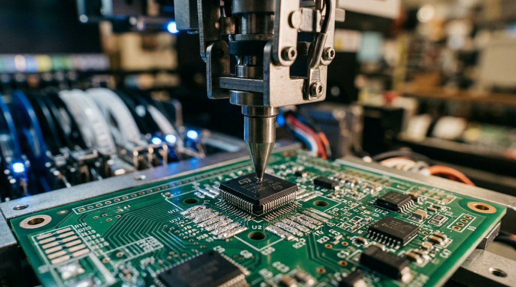
Executive Summary: Key Takeaways for High-Intent B2B Electronics Manufacturing
In 2026, the electronics manufacturing ecosystem in the United States demands absolute precision, compressed development cycles, and high-fidelity reliability. Hardware engineering teams and enterprise OEMs require rapid turnarounds on complex builds without sacrificing structural integrity. As a leading professional manufacturer in China, Hitech delivers high-performance Customized PCB Assembly solutions engineered specifically to address these modern bottlenecks. Backed by exceptional after-sales service and guaranteed timely delivery, Hitech enables seamless integration of global production power with local US design engineering standards.
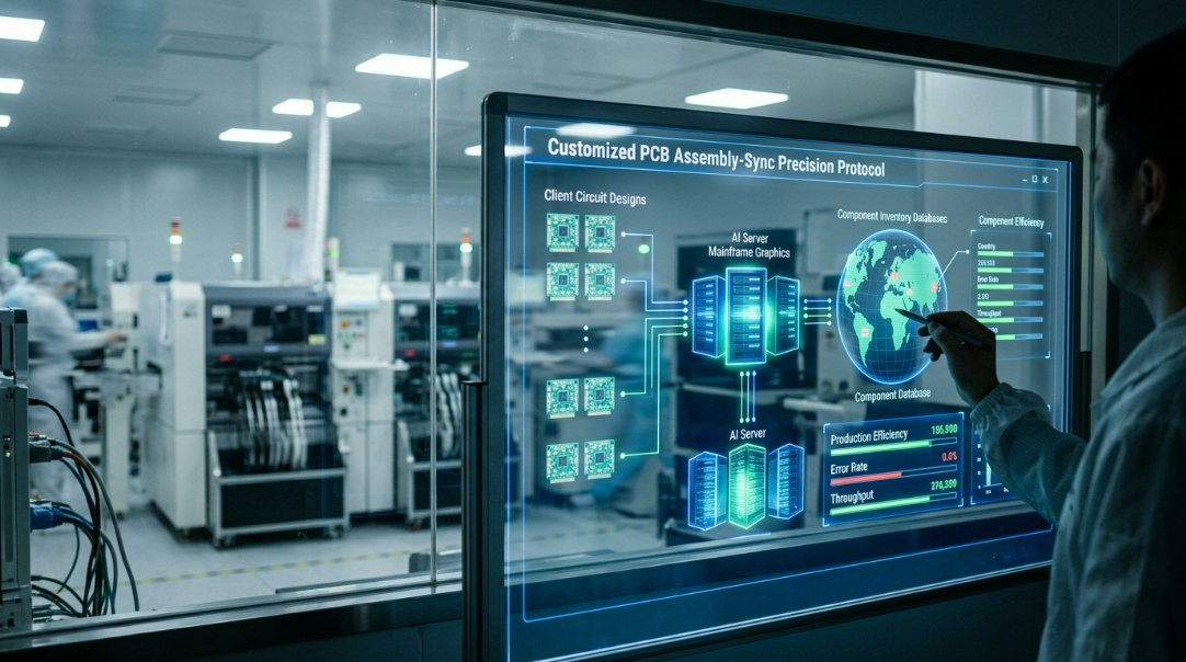
Core Innovation: Leveraging the Proprietary Customized PCB Assembly-Sync Precision Protocol for Real-Time Sourcing
Component availability and dynamic supply chain variations have historically plagued hardware development timelines. To solve this, Hitech has engineered the proprietary Customized PCB Assembly-Sync Precision Protocol. This system serves as a real-time software-to-hardware pipeline, instantly linking client designs with our global parts inventory and primary component distributors. By integrating our deep fabrication intelligence directly with our AI quoting engine, the Customized PCB Assembly-Sync Precision Protocol identifies out-of-stock components, suggests functional pin-compatible alternatives, and optimizes production spacing automatically. The result is a highly predictable, risk-mitigated supply chain that ensures your custom electronics move from design to physical assembly without administrative delays.
Practical Step-by-Step Tutorial: Seamless Customized PCB Assembly Process
Executing a successful production run requires systematic validation at every phase. Below is our engineered step-by-step assembly framework to guarantee optimal hardware execution:
-
Step 1: Uploading Designs into the Interactive 3D Gerber Viewer for Instant DFM Checks
Your project begins by securely uploading your design files (ODB++ or Gerber formats) to Hitech. Our cloud-based interface immediately renders your layout in an interactive 3D viewer. Concurrently, automated Design for Manufacturability (DFM) checks scan trace clearances, drill holes, and physical layer stackups to flag potential errors before production begins. -
Step 2: Utilizing Automated AI-Driven Quoting Tools for Real-Time Component Availability
Our platform parses your Bill of Materials (BOM) instantly. Leveraging the Customized PCB Assembly-Sync Precision Protocol, the system fetches real-time pricing and stock levels. Any single-sourced components with long lead times are highlighted, allowing you to select approved drop-in alternatives on the fly. -
Step 3: SMT Pick-and-Place Setup and Advanced Reflow Soldering Optimization
Once approved, designs are routed to our physical facility. Advanced high-speed surface mount technology (SMT) equipment accurately places passive and active components down to the sub-millimeter level. Reflow ovens are carefully calibrated to establish exact thermal profiles, safeguarding delicate microcontrollers and preventing thermal stress. -
Step 4: Conformal Coating Application and 4-Step Waterproofing Resealing Tutorial
To safeguard designs operating in harsh environments, we perform a dedicated waterproofing cycle: 1) Thorough solvent cleaning of surface impurities; 2) Spraying automated acrylic or silicone conformal coatings; 3) Targeted thermal or UV curing; 4) Mechanical gasket integration to ensure your enclosure assembly holds an active IP67/IP68 rating.
Technical Comparison Matrix: Standard FR4 vs. Flexible Polyimide for RGBIC LED Applications
Selecting the optimal substrate is critical for heat management, mechanical wear, and reliability in architectural or automotive LED configurations.
| Specification / Metric | Standard FR-4 Glass-Epoxy | Flexible Polyimide (PI) |
|---|---|---|
| Dynamic Flexing Life | Rigid Only (Static installation) | High-Flex Cycles (Millions of bends) |
| Thermal Performance (Tg) | 130°C - 180°C | 220°C - 360°C (Extreme range) |
| Relative Substrate Cost | Baseline Standard (Cost-effective) | Premium (1.5x to 2x baseline) |
| Optimal Applications | Heavy controller boards, base power panels | Wearables, thin RGBIC strips, aerospace panels |
Specification Guide: Evaluating 2026 Supply Chain Resilience, Costs, and Voltage Options
Integrating flexible elements or opting for multi-layer FR-4 depends largely on volume and spatial parameters. Standard FR-4 offers unmatched rigidity and physical support for heavy power routing up to several hundred volts. Polyimide offers incredible heat dissipation and space savings, helping US product managers optimize enclosure sizes and reduce final shipping costs, while maintaining strong reliability under dynamic stress.
Electrical Calculation Guidance: Power Supply Load Formulas and Trace Width Calculations for Custom Lengths
Proper electrical calculation is paramount to preventing board failures, trace separation, and excessive heating under heavy electrical load. The IPC-2152 standard details the mathematical relationship for safe current routing:
// STEP 1: Determine Solder Trace Area (A in mil^2)
Area (A) = ( Current (I) / (k * (Temp_Rise (dT)^0.44)) )^(1 / 0.725)

Where:
- I = Operating Current in Amps (e.g. 6.5A)
- dT = Target temperature rise in °C (typically 15°C)
- k = Constant (0.048 for external traces, 0.024 for internal traces)

// STEP 2: Extract Target Trace Width (W in mils)
Width (W) = Area (A) / ( Thickness (T) * 1.37 )

Where:
- T = Copper weight (1 oz copper standard = 1.37 mils)
Using these equations protects physical components from thermal deterioration and guarantees stable, continuous power delivery to downstream microcontrollers and LED arrays.
USA & International Compliance: Meeting UL, CE, FCC, RoHS, IP67/IP68 Flex Certification, and IPC-A-610 Standards
Selling electronic consumer and industrial devices within the United States demands absolute compliance with international regulatory bodies. Every Customized PCB Assembly processed through Hitech is designed and built to clear these certification hurdles. We enforce strict lead-free materials in compliance with RoHS, build to IPC-A-610 Class II and III standards for military and aerospace grade reliability, verify trace distances to align with FCC electromagnetic interference shielding, and run pressure chambers to certify IP67/IP68 waterproofing parameters.
Frequently Asked Questions (FAQ): Expert Answers for B2B Hardware Engineers
How do Smart Home ecosystems (Matter standard, Apple HomeKit, Amazon Alexa) impact custom IoT PCB assembly?
Smart Home ecosystems necessitate extremely clean and shielded radio frequency (RF) design blocks. High-frequency wireless modules operating under the Matter protocol (Thread, BLE, Wi-Fi) require exact 50-ohm coplanar waveguide routing and ground plane isolation during assembly to limit noise floor interference and optimize transmitter performance.
What are the exact cutting tolerances, cutting spacing per meter, and panelization clearance requirements?
We work to a standard cutting tolerance of +/-0.1mm on standard boards. Panelization routing spacing requires a minimum clearance of 1.5mm to the closest components. Individual breakaway tabs must be placed every 60mm to 80mm to maintain high mechanical stability while ensuring post-assembly panel singulation is safe and simple.
What are the strict safety instructions and exact wattage calculations for high-voltage power routing?
High voltage operations (over 60V DC) require trace routing creepage and clearance distances calculated under IPC-2221B standards. To calculate safe trace operating wattages (P = I^2 * R), ensure your thermal dissipation metrics do not exceed your material's maximum rated glass transition temperature (Tg), keeping trace heat isolated from sensitive IC pins.
Accelerate Your 2026 Production: Start Your Customized PCB Assembly Project at https://www.hitech-pcba.com/customized-pcb-assembly.html
Ready to streamline your electronics manufacturing and eliminate delays? At Hitech, we bring together deep fabrication experience in China with efficient logistics networks to ship perfectly verified assemblies directly to your dock in the United States. Work with our engineering team today to receive professional, personalized after-sales support and on-time delivery on every order.
Looking for Custom Engineering/OEM Solutions?
As a top-tier professional manufacturer, we deliver direct factory-price solutions for dynamic scaling, engineering projects, and custom systems globally.
Visit Official Website →